| The MBE of the department of Experimental Physics III of Würzburg University (scenes of 1996) |
 |
 |
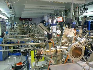
| The impressive system, seen from the load lock used to be a linear setup of four MBE chambers for various semiconductor systems (GaAs, ZnSe, CdTe and HgTe-based). Two additional chambers provided means for in-situ characterization using X-ray Photo-Spectroscopy (XPS) and for contact fabrication by metallization. |
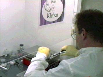
Thomas Schuhmann preparing a GaAs substrate for growth. Following an etching step, the substrate is mounted on a moly-block, a molybdenum template, using Indium which provides a good thermal contact. The moly-block can be íntroduced into the system via the load lock, which is shown below. |
 |
 |
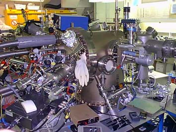
| The ZnSe chamber was used to develop blue-green emitting laser diodes using elemental sources Zn, Cd, Mg and Se, S and the dopants N and ZnCl. I worked with this chamber for three years (1993-1996). My particular interest was the p-type doping of ZnSe using Nitrogen plasma which was produced by a RF-plasma source, the black box seen at the lower left. |
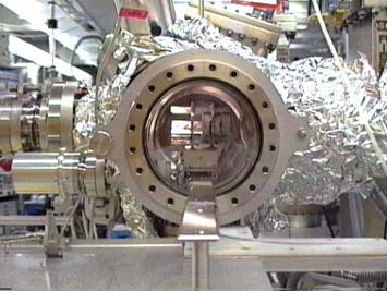
A view into the load-lock, the loading chamber of the MBE system. A cart carrying several moly-blocks is used for transporting the substrates to the various growth chambers. The load-lock is set to normal pressure for sample introduction. For transfering the sample to the following modules the load-lock must be evacuated to a pressure better than 10-8 mbar which is achieved with a turbo-molecular pump. |